Nanotube networks conjured on crystals


The key to instantly assembling intricate networks of nanotubes has been discovered by scientists armed with some of the most sophisticated microscopes in the world. The phenomenon may one-day help create tiny nano-circuits that let electrons pass through nano-pipes instead of along silicon wires.
Erdmann Spiecker and colleagues at Lawrence Berkeley National Laboratory (LBNL) in California, US, along with Wolfgang Jäger at Christian Albrechts University of Kiel, Germany, used several high-powered microscopes to study a nanoscale phenomenon previously observed in the laboratory but not well understood.
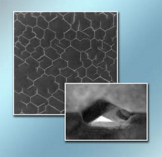
The researchers watched as copper was deposited onto a layered crystal of vanadium selenide, causing complex networks of nano-piping to suddenly pop up on top of the crystal. Each of the nanotubes is 30 nanometres – 30 billionths of a metre – across and together they form roughly hexagonal shapes on top of the crystal, each about 100 nanometres in diameter.
It had been previously suggested that such nano-pipes might be created as cracks form on the crystal surface as the copper layer is applied. But the US-German researchers saw that the nano-pipes actually form when the top layer of the crystal buckles upwards to relieve the molecular strain caused by the deposition of the metal.
Phase change
They used a low-energy electron microscope (LEEM) to observe the vanadium selenide crystal layers during copper deposition. Then they employed another powerful instrument – a high-resolution transmission electron microscope – to watch as the surface structures emerged.
The researchers think the phenomenon depends on the nature of the underlying crystal, which exhibits strong bonds within its layers but weak ones in between layers.
"We believe we are observing a chemical reaction, involving a phase change in the lattice structure of the surface layers," Spiecker says. This “intercalation phase” is when the copper atoms get lodged between the crystal molecules in the surface layer but do not penetrate further. This is thought to create the tension which causes the buckling of the layer to create the tubes.
A better understanding of the phenomenon may someday help material scientists manufacture nano-circuits that channel electrons through tiny tunnels instead of along silicon wires, which have to be etched lithographically. Such circuits would be many times smaller than today's, allowing greater computer power to be packed into chips of the same dimensions.
"Rather relying on lithographic methods, [this technique] exploits some engineered defects that spontaneously form a structure upon processing," says Mark Welland at Cambridge University's Nanoscience Centre in the UK. "Although there is a big step to making a useful device or material, it opens up some interesting possibilities."
Properties:www.newscientist.com

0 Comments:
Post a Comment
<< Home